Intel Tesla TeraFab: The $25 Billion Semiconductor Partnership
Article Content
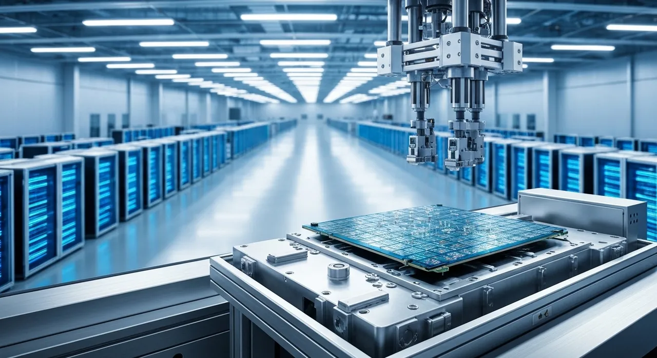
The global semiconductor landscape shifted on its axis on April 23, 2026. In a definitive move that signals the end of the “fabless” era for big tech, Intel and Tesla announced a multi-billion-dollar strategic partnership to anchor the Intel Tesla TeraFab project in Austin, Texas. Estimated to cost between $20 billion and $25 billion, this facility is not merely another factory; it is a “systems foundry” manifest, a vertical monolith designed to unify silicon fabrication, HBM (High Bandwidth Memory) integration, and advanced packaging under a single, massive roof.
For Intel, the deal represents the ultimate validation of its “Foundry 2.0” strategy. After years of struggling with operational losses and yield delays on its 18A node, the 14A (1.4nm-class) process has finally found its “anchor tenant” in Elon Musk. For Tesla, the Intel Tesla TeraFab is the final piece of the vertical integration puzzle, allowing the company to bypass the capacity bottlenecks of TSMC and Samsung to produce its AI5 and future AI6 silicon at a scale never before seen in the Western hemisphere.
Inside the TeraFab: A One-Terawatt Computing Vision
The scale of the Austin facility is difficult to overstate. Musk has claimed the facility will eventually scale to an annual computing output of one terawatt. To put that in perspective, that is nearly double the total current computing capacity of the entire United States. Achieving this requires a fundamental departure from traditional chipmaking logistics. Historically, a chip might be etched in Taiwan, tested in Malaysia, and packaged in mainland China. The TeraFab eliminates this “silicon mileage” by co-locating the entire lifecycle on a single campus near the existing Tesla Gigafactory.
The Intel Tesla TeraFab architecture relies on several “all-under-one-roof” innovations:
- Integrated Lithography: Utilizing the world’s first high-volume fleet of ASML Twinscan EXE:5200 High-NA EUV machines.
- Memory Co-location: Direct integration lines for SK Hynix-sourced LPDDR5X and future HBM4 modules, reducing the latency and cost associated with global shipping.
- Subterranean Logistics: A network of Boring Company tunnels beneath the fab to move sensitive wafers between cleanrooms without atmospheric exposure or vibration-induced defects.
The Technical Heart: Intel’s 14A Process and High-NA EUV
At the center of the partnership is Intel’s 14A process technology, the first node in the industry to move into the “Angstrom Era” using High-NA (High Numerical Aperture) EUV lithography. While rivals like TSMC have publicly stated they will continue to rely on Low-NA multi-patterning until at least 2028 to keep costs down, Intel is taking the expensive leap forward now. This 1.4nm-class node is the primary reason Tesla committed to the project.
The 14A process introduces several key architectural breakthroughs that are critical for Tesla’s power-hungry AI workloads:
1. RibbonFET 2 (GAAFET)
Intel’s second-generation Gate-All-Around (GAA) transistors, known as RibbonFET, provide superior electrostatic control. This allows for higher drive currents at lower voltages, a necessity when your AI inference chips are operating in the thermally constrained environments of a humanoid robot or a self-driving car.
2. PowerDirect (PowerVia 2.0)
Perhaps the most revolutionary aspect of the 14A node is PowerDirect, Intel’s refined backside power delivery system. By moving the power delivery network to the back of the wafer, Intel decouples the power and signal wires. This reduces the “voltage droop” that plagues high-performance AI chips and allows for a 25% to 35% reduction in total power consumption compared to the 18A node. For Tesla, this translates directly into longer range for vehicles and longer operational hours for its Optimus humanoid fleet.
3. Turbo Cells
The 14A node also debuts “Turbo Cells,” specialized high-drive, double-height cells within the standard cell libraries. These are designed to optimize the critical timing paths of the GPU and neural accelerators within the AI5 chip, pushing the maximum frequency beyond what was previously possible on a mobile-grade thermal envelope.
The Silicon: Tesla AI5 and the Move to 1.4nm
The first major product slated for the Intel Tesla TeraFab is the Tesla AI5 processor. This is a radical departure from the HW4 (Hardware 4) systems found in the 2024-2025 Model Y. The AI5 is architected as a half-reticle design, a strategic choice necessitated by the anamorphic lenses of High-NA EUV machines, which halve the exposure field of view. By designing for a single-mask half-reticle, Tesla avoids the complexity and yield-loss of “stitching” two masks together.
Technical specifications for the AI5 manufactured on Intel 14A include:
- Inference Power: Projected 2,500 TOPS (Trillion Operations Per Second), representing a 5x leap over HW4.
- Memory Architecture: Support for up to 192GB of LPDDR5X memory directly on the package, providing a 384-bit memory interface with bandwidth exceeding 1.5 TB/s.
- Functional Deletion: In a move toward “radical simplicity,” Tesla has removed the dedicated Image Signal Processor (ISP) and traditional GPU, moving those functions into a unified AI-inference GPU architecture.
Musk has emphasized that the 14A node will be “prime-time ready” just as the TeraFab hits its initial volume ramp in late 2026. This timeline is aggressive, but the partnership with Intel Foundry provides Tesla with the “Systems Foundry” support it needs—offering not just wafers, but the advanced packaging expertise required to stack logic and memory in a single, high-density module.
Strategic Lifeline: Why Intel CEO Lip-Bu Tan Bet the Farm
For Intel’s CEO, Lip-Bu Tan, the Intel Tesla TeraFab is more than a contract; it is a survival mechanism. Intel Foundry has faced a “valley of death” over the last 24 months, with massive capital expenditures for the CHIPS Act-funded fabs in Ohio and Arizona leading to deep quarterly losses. By securing Tesla as a committed 14A customer, Intel finally has the volume needed to justify the $400-million-per-unit cost of ASML’s High-NA tools.
This partnership also changes the competitive narrative. For years, the foundry market was a two-horse race between TSMC and Samsung. By winning the Tesla contract, Intel has proven that its 14A PDK (Process Design Kit) is stable enough for the world’s most demanding AI customer. This move is expected to trigger a “halo effect,” potentially drawing in other tech giants like Apple or Nvidia, who are increasingly wary of the geopolitical risks associated with Taiwan-centric manufacturing.
Geopolitical and Economic Impact of the Austin Fab
The Intel Tesla TeraFab represents a significant milestone in the re-industrialization of the United States. With the backing of the U.S. CHIPS Act, the project aims to secure a domestic supply of the world’s most advanced processors. The economic impact on the Austin-Round Rock metro area is expected to be profound:
- Direct Employment: The project is slated to create over 10,000 high-tech manufacturing and engineering jobs by 2027.
- Supply Chain Localization: Chemical and substrate suppliers are already reportedly scouting sites in Travis County to be within “Boring distance” of the TeraFab.
- Energy Demands: To power the 1 terawatt compute goal, Tesla is expected to deploy a dedicated “Starlink Power” grid, combining massive solar arrays with Megapack battery storage to ensure the fab remains carbon-neutral.
The sheer power requirements of High-NA EUV lithography—which uses significantly more electricity than previous generations—mean that the TeraFab’s proximity to Tesla’s energy infrastructure is not just a perk, but a technical requirement. The facility is expected to be the largest single consumer of industrial power in the state of Texas by the time it reaches full capacity in 2028.
Conclusion: The Dawn of the TeraFab Era
The announcement of the Intel Tesla TeraFab is the opening salvo in a new era of semiconductor manufacturing. The traditional “division of labor” in the chip industry—where one company designs, another faxes, and another packages—is being replaced by the vertically integrated systems foundry. In this new world, the distinction between a car company, an AI company, and a chipmaker is blurred beyond recognition.
If Intel and Tesla can execute on the 14A roadmap, they will have created a domestic manufacturing moat that is virtually impenetrable. The goal of 100 billion custom AI chips per year is no longer a Muskian “moonshot”—it is a planned industrial reality. As the first 14A wafers begin their journey through the High-NA machines in Austin, the rest of the world’s foundries will be watching closely. The silicon throne is up for grabs, and it is currently being forged in the heart of Texas.
Written by
TempMail Ninja
Digital privacy and online security expert. Passionate about creating tools that protect users' identity on the internet.