Jalapeño AI Chip: OpenAI and Broadcom Launch Custom LLM Accelerator
Article Content
In the rapidly consolidating landscape of artificial intelligence, the physical hardware bottleneck has long been the primary arbiter of scale, cost, and operational viability. On June 24, 2026, OpenAI and Broadcom took a decisive step to break this paradigm by officially unveiling the Jalapeño AI chip—OpenAI’s first custom-designed, proprietary silicon accelerator. Architected specifically as an Application-Specific Integrated Circuit (ASIC) rather than a general-purpose graphics processing unit (GPU), the chip represents OpenAI’s strategic pivot toward hardware-software co-design. This dedicated “Intelligence Processor” is engineered from a blank slate to power the computationally heavy and recurring workloads of Large Language Model (LLM) inference and autonomous agentic AI systems. By transitioning toward custom-built silicon, OpenAI aims to significantly reduce its dependency on general-purpose GPUs, lower the soaring operational costs of running systems like ChatGPT, and scale its global infrastructure sustainably.
To appreciate the engineering milestone of the Jalapeño AI chip, one must understand why inference is a fundamentally different computational problem than training. While training neural networks is highly parallelizable and relies heavily on raw compute density (floating-point operations per second), LLM inference is notoriously constrained by the “memory wall”. In auto-regressive decoding—where models generate tokens sequentially—the speed of generation is strictly limited by how quickly model weights can be loaded from off-chip memory into the processor’s register files. By building a purpose-built ASIC rather than repurposing a training accelerator, OpenAI can optimize the silicon directly around the specific kernels, memory movement, and serving patterns that matter most for modern frontier models.
Breaking the Memory Wall: Under the Hood of the Jalapeño AI chip
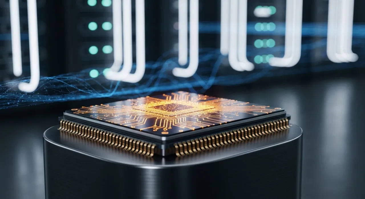
Recent hardware analyses of the physical Jalapeño package reveal a sophisticated, reticle-limited design optimized specifically to maximize data movement efficiency. Manufactured on TSMC’s advanced lithography nodes, the computational die size of Jalapeño is estimated to be approximately 840 mm², approaching the physical limits of extreme ultraviolet (EUV) lithography equipment. This massive footprint represents a packaging scale usually reserved for high-end training clusters, but here it is deployed to maximize on-chip SRAM cache and memory interface density.
According to structural analyses, the physical architecture of the package features:
- Colossal Compute Chiplet: A single, high-density logic tile designed specifically to handle multi-head attention mechanisms, matrix multiplications, and custom transformer kernels.
- Six High-Bandwidth Memory (HBM) Modules: Flanking the central compute die to secure ultra-high-speed memory bandwidth, bypassing the bandwidth limits of standard DRAM and keeping latency to a minimum.
- Integrated I/O Chiplet: Supported by structural dummy dies to manage packaging stress, facilitating ultra-fast die-to-die interfaces and massive scale-out routing.
By tuning this structure directly to dynamic KV-caching (which stores the history of past tokens to speed up subsequent generation) and continuous weight loading, the chip minimizes off-chip data movement. OpenAI’s hardware program, led by Richard Ho, reports that this architectural specialization allows the hardware to run workloads remarkably close to its theoretical peak utilization limit, avoiding the thermal and efficiency losses common in general-purpose architectures.
The Co-Design Ecosystem: Broadcom, Celestica, and TSMC
The realization of the Jalapeño AI chip relied on a robust ecosystem of semiconductor and systems giants to bring the silicon to life. While OpenAI provided the high-level architecture, software profile, and algorithm-level specifications, it partnered with Broadcom to handle silicon implementation and networking. Broadcom integrated its world-class networking heritage directly into the hardware, incorporating its Tomahawk switching architecture (utilizing Tomahawk 6 silicon with throughputs up to 1.6 Tbps). This provides the low-latency, high-bandwidth chip-to-chip scaling needed to cluster these processors into unified compute nodes.
For physical deployment, Celestica was brought in as the hardware systems partner. Celestica is responsible for the board, rack, and system-level integration:
- Custom PCB Layouts: Engineering high-density printed circuit boards that house the processor and support massive power distribution networks.
- Modular Server Racks: Designing custom chassis optimized for energy efficiency and thermal dissipation.
- Liquid-Cooling Integration: Implementing liquid-cooling paths directly into the server racks to manage the immense heat densities associated with continuous, high-frequency inference workloads.
This end-to-end integration ensures that when the chips are deployed in massive data center clusters, they operate stably at high frequencies under continuous operational loads.
The Nine-Month Generative Design Loop
In the semiconductor industry, custom high-performance ASICs typically take 18 to 36 months to go from initial concept to manufacturing tape-out. The complexity of routing billions of transistors, verifying logical blocks, and simulating thermal behavior across multi-die packages usually requires multiple iterative design loops. However, OpenAI and Broadcom co-developed Jalapeño in an exceptionally fast nine-month design cycle. This unprecedented acceleration was achieved by utilizing OpenAI’s own advanced generative models to automate, simulate, and optimize the silicon design process.
By deploying reinforcement learning agents and specialized coding models, OpenAI’s engineering teams automated several key design tasks:
- RTL Generation: Accelerating Register-Transfer Level coding for specialized architectural blocks, cutting down manual coding time by orders of magnitude.
- Physical Placement and Routing: Optimizing the physical layout of billions of transistors to minimize latency and electrical resistance across the 840 mm² compute die.
- Logical Verification: Automating the generation of synthetic testing environments to discover logic errors and physical defects before physical fabrication.
This self-referential design loop proves that generative AI is not just a software phenomenon; it is actively accelerating the physical engineering cycles of the hardware required to sustain it.
Empirical Lab Testing: Running GPT-5.3-Codex-Spark
The Jalapeño AI chip is already a functional reality in the laboratory. Active engineering samples are currently running machine learning workloads at production-target frequencies and power envelopes. Among the first frontier workloads running on the silicon is GPT-5.3-Codex-Spark, an upcoming highly advanced coding and reasoning model.
While OpenAI is still measuring final benchmarks ahead of a detailed technical report, early lab testing indicates that Jalapeño delivers a performance-per-watt ratio substantially better than today’s state-of-the-art accelerators, such as Nvidia’s Blackwell-generation GPUs. Sources close to the project report that the chip can reduce inference operational costs by up to 50%. This efficiency is highly critical for complex reasoning models that require long-running, multi-turn cognitive loops. By maintaining high throughput alongside low latency, the chip ensures that advanced intelligence remains accessible without hitting a physical power or cost wall.
The Macroeconomics of Inference and the De-Nvidiaization of AI
To understand the strategic importance of the Jalapeño AI chip, one must look at the shifting economics of generative AI. While training a frontier model is a massive one-time expense, serving that model to hundreds of millions of users daily generates an astronomical, compounding recurring cost. This financial pressure is magnified by the transition to agentic AI.
Unlike simple chatbots, autonomous agents operate in continuous loops—calling APIs, executing code, and self-correcting. This can increase the demand for token generation by up to 24 times per user session. Running these token-heavy workloads on general-purpose commercial GPUs is unsustainable. By internalizing its core computing infrastructure, OpenAI is pursuing full-stack vertical integration, reminiscent of Apple’s transition to its own silicon. This strategy provides massive economic advantages:
- Supply Chain Autonomy: Bypassing market markups, chip allocation caps, and supply constraints from external vendors.
- Custom Kernel Tuning: Matching silicon capabilities directly to proprietary software kernels, maximizing realized utilization.
- Resource Efficiency: Maximizing the physical utilization of expensive memory and silicon die area, keeping thermal envelopes manageable.
By deploying proprietary, highly efficient silicon, OpenAI ensures it can offer advanced agentic intelligence at scales and prices that are physically impossible for competitors relying solely on off-the-shelf hardware. This movement signifies that following Google (TPU), Amazon Web Services (AWS Trainium), and Meta (MTIA), OpenAI has successfully established its presence in the in-house custom chip frontline.
Gigawatt-Scale Deployment and the Road to 2029
The launch of the Jalapeño AI chip marks the first step of a multi-generation infrastructure roadmap of staggering scale. OpenAI and Broadcom have outlined plans to begin initial deployments of the new computing platform starting in the second half of 2026. These deployments will occur in partnership with primary infrastructure providers, most notably Microsoft, integrating the custom ASICs directly into their global Azure data center networks.
The scale of this infrastructure initiative is defined in gigawatts. The strategic agreement between OpenAI and Broadcom envisions the rolling deployment of up to 10 gigawatts of custom AI accelerators and specialized networking systems by the end of 2029. To put this in perspective, 10 gigawatts of power capacity is equivalent to the output of several large nuclear power plants, reflecting the gargantuan physical footprint required to power the global transition toward artificial general intelligence.
By aligning this massive physical expansion with proprietary, highly efficient silicon, OpenAI is building a moat that extends far beyond software. A custom chip that is 50% cheaper to operate and significantly more energy-efficient allows OpenAI to offer API pricing, real-time reasoning, and agentic capabilities at scales and price points that are functionally impossible for competitors relying solely on off-the-shelf hardware. Jalapeño is the key that unlocks this future—a physical testament to the fact that in the age of AI, the ultimate winners will be those who control the stack from the mathematical algorithms all the way down to the physical silicon.
Written by
TempMail Ninja
Digital privacy and online security expert. Passionate about creating tools that protect users' identity on the internet.