Intel 80386 Microcode Disassembled: 40-Year-Old Bug Revealed
Article Content
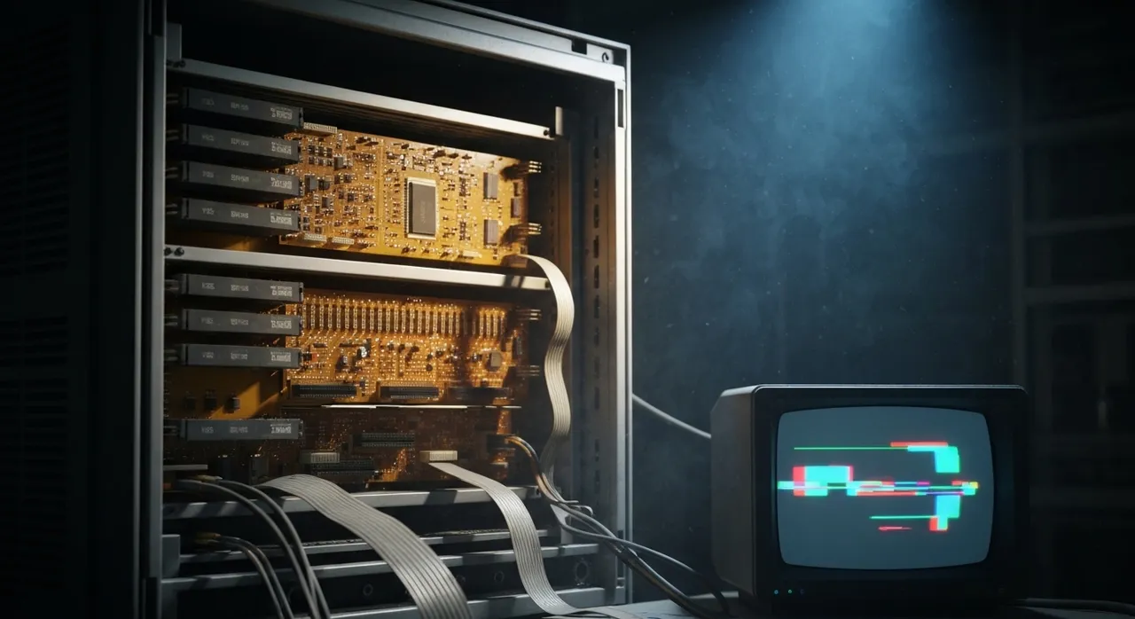
In the history of personal computing, few processors carry the legacy of the Intel 80386. Launched in 1985, this 32-bit milestone introduced paging, flat memory addressing, and robust protected-mode multitasking, establishing the physical foundation for modern operating systems like Windows, OS/2, and Linux. For decades, the lowest-level execution routines of this legendary processor remained locked away in silicon, a proprietary black box. That changed with a historic milestone in hardware archaeology: a collaborative group of demoscene veterans and silicon archivists successfully extracted, corrected, and disassembled the original Intel 80386 microcode, revealing how the chip controls its internal units and uncovering a 40-year-old hardware bug in the process.
The breakthrough is the result of a coordinated effort by software developers and chip historians. Renowned archivist Ken Shirriff provided high-resolution die photographs of the 80386’s microcode ROM. Using image processing, machine learning classification, and manual verification, researchers Daniel Balsom (famed as “gloriouscow”), Smartest Blob, and nand2mario extracted and reconstructed the physical bits from the silicon. Democoder and retro-computing pioneer reenigne (Andrew Jenner, creator of the legendary IBM PC demo “8088 MPH”) then analyzed the raw data, mapped the processor’s 37-bit-wide microinstructions, and identified 215 distinct microcode entry points. This masterclass in reverse engineering has provided the computing world with two monumental discoveries: a previously undocumented security vulnerability inside the 386’s I/O protection logic, and a fully functional, cycle-accurate replica of the processor running on modern FPGA hardware.
Unlocking the Intel 80386 Microcode
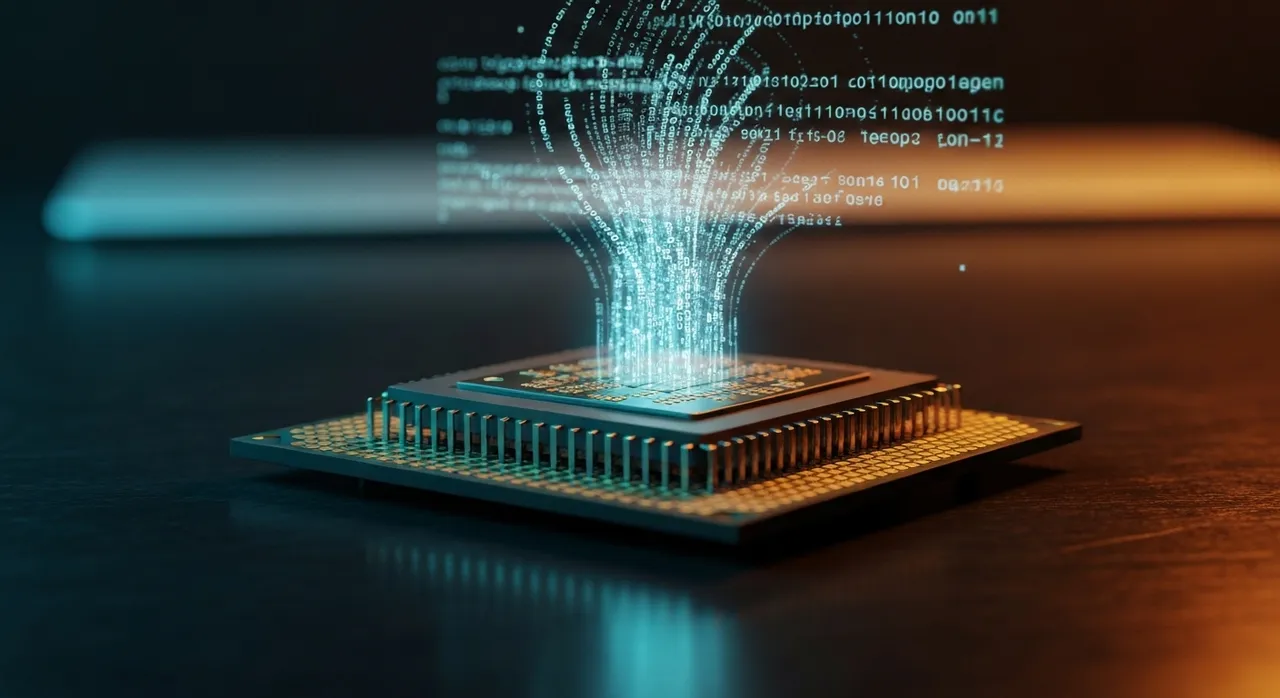
The scale of the 80386’s internal logic represented a massive leap in microarchitectural complexity over its 16-bit predecessor, the 8086. While the 8086’s microcode control store comprised a modest 10,752 bits, the Intel 80386 microcode ROM holds a staggering 94,720 bits, organized into 2,560 words of 37 bits each. This massive control program was a complete black box. Unlike the 8086, which had documented patents that provided hints to its microcode structure, the 80386 had no public blueprints. The team had to reverse-engineer the microinstruction format from scratch.
To decode the 37-bit-wide words, the researchers used Python scripts to convert the extracted bit arrays into 37-pixel-wide bitmaps. By analyzing these long, thin images, they identified vertical patterns that hinted at the boundaries of individual microcode fields. They mapped these visual structures against the processor’s match-decoder Programmable Logic Array (PLA). Because the PLA maps x86 instruction opcodes to specific starting locations in the microcode ROM, knowing these starting positions helped the team match individual instructions with their corresponding microcode sequences.
The team looked for instructions with highly predictable behavior to verify their theories. For instance, instructions like PUSHA (Push All General-Purpose Registers) and POPA (Pop All General-Purpose Registers) are implemented as loops in microcode, which step through registers in a fixed sequence. Identifying the microcode loops that incremented these register indexes allowed the team to confirm the exact bit-fields used to select internal registers. Through this process, they gradually decoded the entire instruction set.
Deciphering the 37-Bit Microinstruction Word
The disassembly revealed that each 37-bit microinstruction is structured as a vertical microcode word. Rather than controlling every logic gate directly, the 80386 uses highly encoded fields that are routed to internal hardware accelerators, such as the dedicated barrel shifter and the hardware multiply/divide unit. Reenigne divided the 37-bit microcode word into the following key execution fields:
- Source (src): Selects the register or internal datapath endpoint providing the operand.
- Destination (dest): Selects the register that will receive the output of the operation.
- ALU Source (alu_src): Selects the second operand for the Arithmetic Logic Unit.
- ALU/Jump Op: Encodes either the specific arithmetic operation or a branch target for the microcode sequencer.
- Sub-Op (sub): Manages sequencer behavior, loop flags, and operand sizing (handling 8-bit, 16-bit, and 32-bit operations dynamically).
- Bus: Triggers memory reads, writes, prefetch flushes, or descriptor-cache modifications.
Because the 386 was optimized for speed, its microcode is designed to interact with hardware state machines. For example, the microcode does not implement complex page-table walking or segment validation in software; instead, it writes configuration values to dedicated hardware units (such as the Protection PLA or the Paging Unit) and allows those units to handle the execution in parallel.
The 40-Year-Old Security Glitch: Bypassing I/O Protection
The most surprising discovery of the disassembly is a hardware flaw within the 80386’s input/output (I/O) port protection logic. In protected-mode operating systems, the kernel restricts user-space (Ring 3) applications from accessing raw hardware ports. To grant specific programs access to hardware (such as a graphics card or sound card), the operating system uses the I/O Permission Bitmap, which is stored in the Task State Segment (TSS). This bitmap contains one bit for each of the 65,536 possible I/O ports; a 0 bit allows access, while a 1 bit blocks it.
When an application executes an I/O instruction (like IN or OUT), the processor’s microcode must check this bitmap. Because I/O ports can be accessed in widths of 1 byte, 2 bytes, or 4 bytes, the microcode must verify that all bytes of the target port range are authorized. For example, if a program attempts a 4-byte (32-bit) access to port 0x3F8, the CPU must check the permission bits for ports 0x3F8, 0x3F9, 0x3FA, and 0x3FB.
The disassembled microcode reveals that the 80386’s validation routine contains a classic “off-by-one” boundary error. When a 4-byte port access is initiated, the microcode only validates the permission bitmap for the first three port addresses. If a program executes a 4-byte access at the very edge of its allowed range, the check for the fourth and final byte is skipped entirely. This allows the user-space program to read from or write to the unauthorized fourth port without triggering a General Protection Fault (#GP).
Through this bypass, a user-mode process can access sensitive, protected system registers (such as interrupt controllers, system timers, or DMA controllers) that the operating system intended to shield. It is extremely rare for a security vulnerability in such a historically ubiquitous piece of hardware to remain undetected for over forty years. Because the flaw is hardwired into the CPU’s silicon ROM, it cannot be patched via software, making it a permanent characteristic of original 80386 hardware.
z386: Synthesizing the Microcode into Verilog
Armed with the fully decoded Intel 80386 microcode, developer nand2mario created the z386 project—an open-source, hardware-description-language (HDL) implementation of the 80386 CPU in SystemVerilog. Unlike typical FPGA-based PC emulators (like the popular ao486 core), which emulate x86 instructions using modern, custom-designed pipelines, z386 is built around the original 386 microcode.
Instead of writing complex Verilog state machines to execute instructions like ADD, IRET, or SGDT, nand2mario constructed the physical execution units that the original microcode expects to manipulate. This includes recreating the prefetch queue, the two-pass PLA-based instruction decoder, the 32-entry Translation Lookaside Buffer (TLB), the segment caches, the barrel shifter, and the microcode sequencer itself. When z386 runs, the recovered 37-bit microcode control program drives the virtual wires of the FPGA exactly as it did on original Intel silicon in 1986.
This approach has proven to be incredibly robust. Because the core uses the exact microcode routines of the original processor, it inherits 100% of the 386’s real-world behavior. The z386 core successfully boots MS-DOS 6.22 and FreeDOS, runs protected-mode DOS extenders (such as DOS/4GW and DOS/32A), and plays legendary 32-bit software titles like *DOOM* and *DOOM II* on FPGA hardware.
Comparing z386 and ao486 on FPGA
The difference in design philosophy between z386 (a microcode-accurate 386) and ao486 (a high-level, pipelined 486-class core) is clearly visible when comparing their hardware utilization and performance on a DE10-Nano FPGA board:
- Code Complexity: By relying on the recovered microcode ROM to define instruction behavior,
z386requires only 8,000 lines of SystemVerilog code, compared to the 17,600 lines required byao486. - Silicon Efficiency:
z386uses fewer FPGA logic resources, requiring 18,000 Adaptive Lookup Tables (ALUTs) and 5,000 registers, whereasao486demands 21,000 ALUTs and 6,500 registers. - Execution Speed: While
z386runs at a comparable clock speed on the DE10-Nano (85 MHz versusao486‘s 90 MHz), its real-world performance in *DOOM* is slightly lower, yielding 16.5 frames per second compared toao486‘s 21.0 frames per second.
This performance gap highlights the trade-offs of microarchitectural accuracy. The original 80386 is a highly serialized processor. For example, a simple register-to-register move instruction takes two clock cycles because the microcode requires one cycle to pass the value through the ALU and a second “delay slot” cycle to write the result back to the target register. The ao486 core bypasses this bottleneck by utilizing a more modern, pipelined RISC-like architecture that executes more instructions per clock cycle (lower CPI). However, for purists, historians, and systems developers, z386 represents a major achievement: a truly accurate recreation of the processor that defined 32-bit personal computing.
A Monument to Hardware Archaeology
The disassembly of the Intel 80386 microcode represents a milestone for legacy systems preservation. By extracting and documenting the 94,720 bits of the 386’s control ROM, this collaborative project has turned a legendary piece of closed silicon into an open-source educational resource. It has demonstrated that even after forty years, legacy hardware still holds hidden secrets—from subtle off-by-one security vulnerabilities to elegant hardware-software co-designs that allowed 1980s chips to accomplish complex tasks on a tiny transistor budget. Through the work of these reverse engineers, the digital DNA of the 32-bit era has been preserved for generations of computer scientists to study, replicate, and run.
Written by
TempMail Ninja
Digital privacy and online security expert. Passionate about creating tools that protect users' identity on the internet.