Google Marvell AI chips: Advanced Talks for Custom AI Processor Development
Article Content
The Silicon Sovereignty Shift: Decoding the Google-Marvell Partnership for Custom AI Chips
On April 19, 2026, the landscape of hyperscale computing underwent a seismic shift as reports emerged that Alphabet’s Google is in advanced negotiations with Marvell Technology to co-develop two new specialized processors. This high-stakes collaboration, centered on Google Marvell AI chips, represents more than just a hardware refresh; it is a definitive strategic pivot aimed at dismantling the “NVIDIA tax” and preparing Google’s global infrastructure for the era of agentic AI. As large language models transition from research curiosities to autonomous enterprise agents, the bottlenecks have shifted from raw compute power to memory efficiency and inference economics.
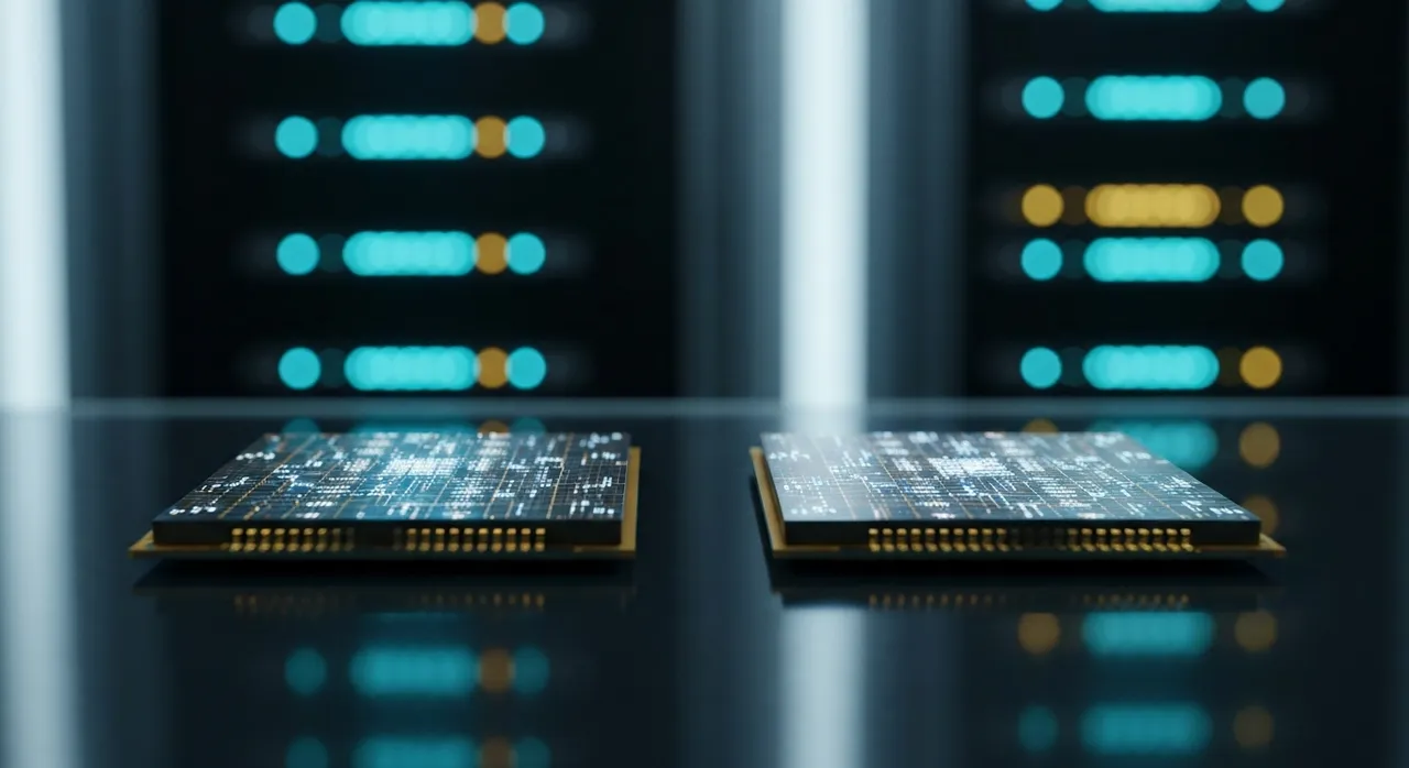
The proposed deal involves two distinct pieces of silicon: a first-of-its-kind Memory Processing Unit (MPU) and an updated, inference-optimized version of Google’s Tensor Processing Unit (TPU). For Google, which has historically relied on Broadcom for its flagship TPU designs and MediaTek for its cost-sensitive “e” variants, the inclusion of Marvell signifies a tactical diversification of its supply chain. By bringing Marvell into the fold—a company with a $1.5 billion annual run rate in custom silicon and deep roots in networking and high-speed data interconnects—Google is signaling that the next frontier of AI competition will be won not in the training lab, but in the efficiency of the inference-ready data center.
Breaking the Memory Wall: The Rise of the Memory Processing Unit (MPU)
The most technically significant aspect of the Google Marvell AI chips partnership is the development of the Memory Processing Unit (MPU). In the current 2026 hardware cycle, the industry has hit what engineers call the “Memory Wall.” While compute throughput (FLOPS) has scaled exponentially, the speed at which data can be moved from memory to the processor has lagged behind, creating a massive latency bottleneck for frontier models like Gemini 2.0.
The MPU is designed to sit alongside existing TPUs to handle memory-centric operations that typically clog the main accelerator’s pipeline. According to technical specifications leaked during the negotiations, the MPU will leverage in-memory processing (PUM) techniques to perform the following tasks directly on or near the memory die:
- Activation Quantization: Dynamically scaling data precision to reduce the memory footprint without losing model accuracy.
- Gather/Scatter Operations: Efficiently managing sparse data structures common in Mixture-of-Experts (MoE) architectures.
- Prefetching and Compression: Reducing host-to-accelerator bandwidth pressure by preparing data before the compute core requests it.
By offloading these “housekeeping” tasks to a dedicated Marvell-designed MPU, Google expects to achieve up to a 3x increase in inference throughput. This is critical for agentic AI, where models must maintain long-term memory and execute multi-step reasoning loops in real-time. Industry analysts suggest that Google plans to produce approximately 2 million MPU units in the initial ramp-up, targeting a 2027 full-scale deployment.
Diversifying the TPU Stack: Why Marvell?
For over a decade, Broadcom has been Google’s primary design partner, securing a long-term agreement through 2031 for high-performance TPU variants. However, as the custom AI chip market is projected to reach $118 billion by 2033, Google cannot afford single-vendor dependency. Marvell brings a unique set of capabilities to the table, particularly in optical interconnects and chiplet-based architectures.
The second chip in the negotiation is a next-generation TPU specifically engineered for the “inference” phase. Unlike the training-heavy TPU v7 (Ironwood), which scales to 9,216 liquid-cooled chips per superpod, the Marvell-collaborated TPU focuses on performance-per-watt and Total Cost of Ownership (TCO). This chip is rumored to be targeting a 44% lower TCO compared to NVIDIA’s latest Blackwell-successor systems, providing Google Cloud with a massive margin advantage for its enterprise clients.
The Agentic AI Era: Hardware Built for Autonomy
The timing of the Google Marvell AI chips discussions coincides with the industry-wide transition from “Generative AI” to “Agentic AI.” While generative models respond to prompts, agentic systems pursue goals—planning, executing code, and interacting with external tools. This shift fundamentally changes the compute profile of the data center.
- Always-Resident Models: Unlike batch processing, AI agents require models to be “always-on” and resident in High Bandwidth Memory (HBM), necessitating chips with massive memory capacity (targeting 192GB+ per node).
- Tool-Calling Latency: When an agent calls an API or searches a database, every millisecond of “thought-trace” latency compounds. The MPU-TPU duo is designed to minimize this “reasoning overhead.”
- Token Economics: As agents perform thousands of background tasks per user request, the cost per token must drop by orders of magnitude for the business model to remain viable. Custom ASICs (Application-Specific Integrated Circuits) are the only way to achieve this.
Google’s Gemini models are increasingly moving toward this agentic framework. By internalizing the hardware production of these specialized chips, Google can tune the silicon specifically for the Gemini architecture’s unique Mixture-of-Experts (MoE) routing protocols, a level of optimization that general-purpose GPUs cannot match.
Strategic Impact: Eroding NVIDIA’s Hegemony
While NVIDIA remains the dominant force in AI training with its Vera Rubin architecture and H300 GPUs, the Google Marvell AI chips deal represents a strategic encirclement. As of early 2026, NVIDIA’s market share in the AI accelerator space has begun to settle near 75%, down from its 87% peak in 2024. This decline is largely driven by hyperscalers like Google, Amazon (Trainium/Inferentia), and Meta (MTIA) moving toward internal silicon for inference.
Marvell Technology is positioned as the primary beneficiary of this trend. By securing a design win with Google, Marvell cements its status as the world’s second-most important custom AI chip designer, trailing only Broadcom. Marvell’s ability to integrate its NVLink Fusion and high-speed DSP (Digital Signal Processing) technology into Google’s infrastructure makes it an indispensable partner for the next decade of cloud scaling.
Furthermore, the collaboration puts pressure on NVIDIA to continue lowering the barrier for its own software stack, CUDA. However, Google’s OpenXLA compiler and the maturity of its TPU software ecosystem have now reached a point where migrating from NVIDIA to custom silicon is no longer a multi-year engineering hurdle, but a standard operational choice for Google Cloud customers like Anthropic.
The Road to 2027: Production and Scaling
If the negotiations are finalized by mid-2026, the timeline for the Google Marvell AI chips suggests a prototype phase in early 2027, with mass production scaling in the latter half of that year. The chips are expected to be manufactured using TSMC’s 3nm (N3P) process, with a roadmap toward 2nm transition by 2028. This would put Google’s custom silicon on the leading edge of fabrication technology, parity with the most advanced mobile and desktop processors in the world.
The scale of production is equally ambitious. With Google already committed to producing millions of units of its Ironwood series, the additional 2 million MPUs co-developed with Marvell will fill the gap in “Inference-as-a-Service” capacity. This will allow Google to offer tiered compute pricing: premium NVIDIA-based instances for general-purpose research and highly optimized, low-cost TPU+MPU instances for high-volume agentic workflows.
Conclusion: The Dawn of Vertical AI Integration
The reported partnership between Google and Marvell is a clear indicator that the “commodity” era of AI hardware is ending. In its place is an era of vertical integration, where the software architects of the world’s most advanced AI models are also the designers of the electrons that power them. By developing the Google Marvell AI chips, Alphabet is protecting itself against supply chain volatility, reducing its capital expenditure in the long run, and creating a specialized environment where Gemini can outperform any model running on generic hardware.
For the broader market, this deal is a signal to investors and competitors alike: the race for AI dominance is no longer just about who has the most GPUs—it is about who can design the most efficient memory and inference systems to sustain the agentic AI revolution. As Marvell and Google move toward a formal agreement, the message to the semiconductor industry is clear: specialization is the only path to survival in the multi-trillion-dollar AI economy.
Written by
TempMail Ninja
Digital privacy and online security expert. Passionate about creating tools that protect users' identity on the internet.